Difference between revisions of "SHA-3 Hardware Implementations"
(→High-Speed Implementations (FPGA)) |
|||
| Line 47: | Line 47: | ||
| Grøstl-384/512 || Submission document || [[#Fully_Autonomous_Implementation|Fully autonomous]] || P & Q permutation in parallel || Xilinx Virtex 5 || align="right"| 5419 slices || align="right"| 15395 Mbit/s || align="right"| 210.5 MHz | | Grøstl-384/512 || Submission document || [[#Fully_Autonomous_Implementation|Fully autonomous]] || P & Q permutation in parallel || Xilinx Virtex 5 || align="right"| 5419 slices || align="right"| 15395 Mbit/s || align="right"| 210.5 MHz | ||
|- | |- | ||
| − | | MD6 || Submission document|| Compression function only, 16 parallel steps || Xilinx Virtex-II Pro || align="right"| 5313 slices || align="right"| 1232 Mbit/s || align="right"| 150.3 MHz | + | | MD6 || Submission document || [[#Implementation_of_Core_Functionality|Core functionality]] || Compression function only, 16 parallel steps || Xilinx Virtex-II Pro || align="right"| 5313 slices || align="right"| 1232 Mbit/s || align="right"| 150.3 MHz |
|- | |- | ||
| − | | MD6 || Submission document|| Compression function only, 32 parallel steps || Xilinx Virtex-II Pro || align="right"| 7529 slices || align="right"| 1894 Mbit/s || align="right"| 141.6 MHz | + | | MD6 || Submission document || [[#Implementation_of_Core_Functionality|Core functionality]] || Compression function only, 32 parallel steps || Xilinx Virtex-II Pro || align="right"| 7529 slices || align="right"| 1894 Mbit/s || align="right"| 141.6 MHz |
|} | |} | ||
Revision as of 13:43, 7 November 2008
Contents
1 Important Information
This page tries to summarize the key properties of reported hardware implementations of the SHA-3 candidates. The implementations are categorized into FPGA and standard-cell ASIC implementations.
Note that the diversity of implementation approaches, target technologies, and synthesis tools makes direct comparisions between different hardware implementation difficult. The more of these parameters agree, the more reasonable the comparison becomes.
The target technology should be as similar as possible. For FPGA implementation, it is desirable to compare implementations on the same target device (or at least on devices of the same FPGA family). For standard-cell ASIC implementation, at least the minimal gate length of the process (e.g., 0.13 µm) should agree. More ideally, the implementations should use the same standard-cell library (which implies the use of the same process technology).
In order to facilitate the comparision of hardware modules with different implementation approaches, we classify them into three categories.
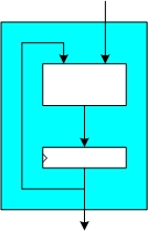
1.1 Fully Autonomous Implementation
Such hardware implementations include the complete functionality of a SHA-3 candidate (or a specific version thereof). That means the input message can be loaded piecewise into the hardware module and it delivers the message digest as output. All hash calculations happen exclusively within the hardware module. If integrated in a system, the achievable throughput of a fully autonomous implementation depends on the speed of the hardware module itself and the speed of the (system dependent) data interface delivering the input message.
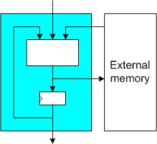
1.2 Implementation with External Memory
These implementations use external memory to hold intermediate values during the hashing of a message. The implemented hardware itself normally consists of the core logic functionality of the hash function, some registers for short-lived temporary values, and possible a memory controller for access to the external memory. Such implementations can load the input message either over a dedicated interface (similar to a fully autonomous implementation) or from the external memory. In order to reach the maximal throughput of the hardware module, the external memory must be sufficiently fast.
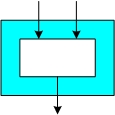
1.3 Implementation of Core Functionality
Such implementations comprise only important parts of the hash function (e.g., the compression function), which normally allows to get a first-order estimate of the performance figures of full implementations.
2 High-Speed Implementations (FPGA)
Important note: The size and fuctionality of slices varies between FPGA families. A direct comparision of the slice count of implementations on different FPGA families is therefore problematic.
| Hash Function Name | Reference | Impl. Approach | Impl. Details | Technology | Size | Throughput | Clock Frequency |
|---|---|---|---|---|---|---|---|
| Grøstl-224/256 | Submission document | Fully autonomous | P & Q permutation in parallel | Xilinx Spartan 3 | 6582 slices | 4439 Mbit/s | 86.7 MHz |
| Grøstl-224/256 | Submission document | Fully autonomous | P & Q permutation in parallel | Xilinx Virtex 5 | 1722 slices | 10276 Mbit/s | 200.7 MHz |
| Grøstl-384/512 | Submission document | Fully autonomous | P & Q permutation in parallel | Xilinx Spartan 3 | 20233 slices | 5901 Mbit/s | 80.7 MHz |
| Grøstl-384/512 | Submission document | Fully autonomous | P & Q permutation in parallel | Xilinx Virtex 5 | 5419 slices | 15395 Mbit/s | 210.5 MHz |
| MD6 | Submission document | Core functionality | Compression function only, 16 parallel steps | Xilinx Virtex-II Pro | 5313 slices | 1232 Mbit/s | 150.3 MHz |
| MD6 | Submission document | Core functionality | Compression function only, 32 parallel steps | Xilinx Virtex-II Pro | 7529 slices | 1894 Mbit/s | 141.6 MHz |
3 High-Speed Implementations (ASIC)
| Hash Function Name | Reference | Implementation Details | Technology | Size | Throughput | Clock Frequency |
|---|---|---|---|---|---|---|
| Grøstl-224/256 | Submission document | P & Q permutation in parallel | UMC 0.18 µm | 131 kGates | 4379 Mbit/s | 85.5 MHz |
| Grøstl-384/512 | Submission document | P & Q permutation in parallel | UMC 0.18 µm | 341 kGates | 6225 Mbit/s | 85.1 MHz |
| Keccak | Submission document | Core (round function, state register) & IO buffer | ST 0.13 µm | 48 kGates | 28400 Mbit/s | 500 MHz |
| Keccak | Submission document | Core (round function, state register) only | ST 0.13 µm | 40 kGates | 15000 Mbit/s | 500 MHz |
| MD6 | Submission document | Compression function only, 48 parallel steps | GPDSK 90 nm | 145 kGates | N/A | 200 MHz |
| MD6 | Submission document | Compression function & memory control logic, 16 parallel steps | GPDSK 90 nm | 105 kGates | N/A | 200 MHz |
4 Low-Area Implementations (ASIC)
| Hash Function Name | Reference | Implementation Details | Technology | Size | Throughput | Clock Frequency |
|---|---|---|---|---|---|---|
| Keccak | Submission document | Core using system memory | ST 0.13 µm | 6 kGates | 26 Mbit/s(*) | 100 MHz |
(*) Estimation for 64-bit memory interface based on published performance figures: (1024 bits/permutation) * (100 * 10^6 cycles/s) / (3870 cycles/permutation) = 26.46 * 10^6 bits/s


